Integrity - based innovation in science and technology Home|Favorite|Contact us
Name:Helen.
Tel:+86-755-82720811
E-mail:helen@chinalctech.com
Add:Room 301,Building No.3,Guole Technopark,Lirong Road,Dalang Street,Longhua District,Shenzhen 518110,China.
Online consulting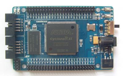
Adopt double deck PCB design, texted by professional circuit board flying, the cirtcuit board is stable and reliable, the power supply and PLL parts dealed withπtype filter. Reference ZhouLiGong experiment box design, using the high cost of tantalum capacitance to do the power filtering processing! Stable and reliable performance, beautiful structure. Supportment FPGA/NIOS II development, all pins can lead out directly from the board to use conveniently, reserved PLL resource.
1. On-board EP2C8Q208C8-FPGA core chip.
2. On-board SDRAM-K4S641632-UC60 or HY57V641620FTP-7 which are compatible with SDRAM, capacity of 64Mbit, independent pins are used to run space of NIOS II experiment program.
3. 50MHz active crystal, provide the system clock work Lord, through the 22 ohm resistance matching connection CLK0 and CLK4 only, can be used as a system clock.
4. 5V power output interface, 5mm external diameters, 5mm inner diameters, positive in, negetive out.
5. Power switch, face the development board, connect the power up.
6. R-C button, FPGA reconfigured buttons, press the button, the system will re-read program from the EPCS4 chip and then continou to work.
7. Rst button can be used as input button, also can be used as system reset button.
8. IN5822 diode to avoid the power reverse connection, high-speed schottky dilde.
9. Power indicator light D2.
10. 25 x2 double row spacing 2.54 user interface.
11. A user LED-D4, independent pin, can not reuse with interfece board.
12. Download indicator light D1, usually light off, will light when download and press the button R-C.
13. JTAG download interface, corresponding to the download document is SOF, fast speed, JTAG download the document directly to FPGA, but the program will be lost without electricity, reconmended you use JTAG mode when study, at last, curing the program can download the program to the configuration chip through ASP mode again.
14. ASP download interface, corresponding to download POF document, it’s lower than JTAG, and need to power uo and polled out the download line, then can work. The operation is more troublesome, not recommented to use when study, finally, the need to power under the condition of the operation to use ASP download mode.
15. 4 wire RS232 serial communication interface and SRAM jump line choice; When connect interface board, change pin and reuse.
16. 25 x2 double row spacing 2.54 user interface.
17. Screw brass pillars support.
18. 1085-3.3V constant voltage chip.
19. 1117-1.2V constant voltage chip, provide FPGA nuclear voltage.
20. SRAM chip IS61LV25616AL 256kx16b (accessories).
21. AT24C02-I2C storage device.
22. Configuration chip EPCS4 (4Mb).
© 2011-2023 Shenzhen LC Technology Co.,Ltd. All rights reserved.
Add:Room 301,Building No.3,Guole Technopark,Lirong Road,Dalang Street,Longhua District,Shenzhen 518110,China.
Tel:+86-755-82720811


Mobile station